Advanced Optical Metrology Solutions for AI Packaging Processes
High-performance advanced packaging—anchored in 2.5D and 3D integration schemes and HBM—has become a key enabler of the AI chips' evolution path. These architectures push performance boundaries, but their growing process complexity makes high-yield manufacturing and long-term reliability increasingly challenging. The following highlights major challenges, solutions, and associated technologies that will be presented.
Wafer-level metrology for post-stacking and bonding in 2.5D integration and HBM. These processes pose serious challenges. For instance, side-by-side packaging of materials with different CTE’s can result with up to 3.5 mm of wafer warpage, while non-uniform die shapes and densities create asymmetric geometries. These deformations can escalate into yield-killing failures such as stress-driven cracks or voids. We’ll demonstrate the use of Spectral Coherence Interferometry technology for wafer- or die-level warpage measurements. This technology enables rapid, direct measurements across the entire wafer with high accuracy, essential for identifying process deviations. Additionally, we will present thickness and Total Thickness Variation (TTV) measurements for complete stacks and individual layers. This is especially critical in HBM manufacturing, where tight stacking tolerances require that each die meets precise thickness specifications to ensure alignment and bonding integrity.
Interconnects and post-CMP and etch metrology in 3DIC. As the industry moves into the next phase of Advanced Packaging, interconnects are being implemented at the silicon level, often on complex multilayered stacks. We will showcase innovative solutions tailored to the most demanding 3DIC and hybrid bonding applications. These solutions offer proven advantages in the inline characterization of critical process elements, including TSVs, Cu Pads, RDLs, and pre-bonding wafer-edge topography. They are based on a unique Spectral Interferometry technique that focuses analysis on reflections from specific regions of interest, filters out deeper-layer contributions, and delivers accurate, robust results through direct measurement.
Illustrations:
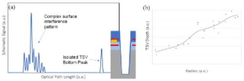
Figure 1
Fig. 1(a) Schematic illustration of Spectral Interferometry data for an individual TSV on a wafer with full back-end processing. Several layers and structures in close proximity to the TSV top create a complex interference pattern. However, the peak originated at the bottom of the TSV is entirely separated from the surface signal, allowing for depth measurement without considering the layers above. Fig. 1(b) Radial distribution of the extracted TSV depth of a wafer with full backend processing. [1]
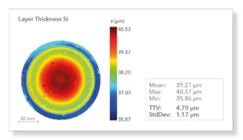
Figure 2
Fig. 2: A High-resolution Silicon Layer Thickness and Total Thickness Variation (TTV) following a back grinding in the W2W Hybrid bonding process using Spectral Coherence Interferometry technology. Such a full-wafer map can reveal details like grinder signatures even after polishing.
References:
[1] S. Schoeche, D. Schmidt, J. Han, S. Butt, K. Sieg, M. Cheng, A. Cepler, S. Dror, J. Ofek, I. Osherov, I. Turovets, "Spectral interferometry for T.S.V.SV metrology in chiplet technology," Proc. SPIE 12955, Metrology, Inspection, and Process Control XXXVIII, 129551O (2024)
Key Technologies Covered
- 2.5D and 3D Packaging
- Die Stacking and Hybrid Bonding
- Die and Wafer Warp/Bow measurement
- Interconnects: TSVs, RDLs, and Cu Pads
- Wafer level metrology
- Wafer Edge Metrology
- Spectral Interferometry
- Spectral Coherence Interferometry
- Optical Scatterometry
- Machine-learning enhanced metrology