移至主內容

Enabling AI systems with atomic-scale precision

上午 10:25 - 上午 10:45

Semiconductor innovation has moved from device-level scaling towards systems-to-materials co-optimization, where compute, memory, interconnect, power, thermal performance, and heterogeneous integration must advance together. Meeting these demands requires new materials and processes capable of delivering higher performance, lower power, tighter variability control, and faster integration across advanced logic, high-bandwidth memory, 3D-architectures, chiplets, and advanced packaging, all of which have come together to enable AI applications. 


This talk explores how advanced materials delivered with atomic-scale precision are becoming essential enablers of the AI era. Deposition and epitaxy technologies – including ALD, PEALD, CVD, and epitaxy – provide the film quality, conformality, interface control, and structural precision needed for next-generation devices and 3D integration.


Key Technologies Covered

  • Advanced materials enabling next-generation logic (e.g., GAA, CFET) and memory (e.g., 4F2 DRAM, HBM, 3D DRAM, etc.) 
  • Advanced deposition processes like ALD, PEALD, epitaxy, CVD
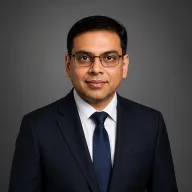
Featured Speakers

Dr. Angada Sachid

Dr. Angada Sachid

Senior Director, ASM

Angada Sachid is a seasoned technologist and engineering leader with over two decades of experience across academia and industry, specializing in advanced semiconductor materials, devices, circuits, and chip design research. He is currently focused on translating device and system inflections into manufacturable materials and process solutions. His work spans front-end innovation and design-technology co-optimization (DTCO), with an emphasis on high-k/metal gate (HKMG) scaling, work-function engineering, variability, advanced-node integration, and new materials.


Before ASM, he held pivotal roles at Intel as a Principal Engineer, Applied Materials as a Director and Distinguished Member of Technical Staff, and a Scientist at the University of California, Berkeley and the Lawrence Berkeley National Laboratory, Berkeley, spearheading research into next-generation semiconductor processes and devices. He received his PhD from the Indian Institute of Technology Bombay in Nanoelectronics. He has authored over 80 publications and patents.